3.3 MOSFET: The Transistor Inside a Tiny Chip
Imagine building an electronic circuit by wiring together transistor components like the one in Figure 3-4 (a). It clearly seems different from the system semiconductors represented by the CPU chip we saw in Figure 1-1. Connect just a few more transistor components, and you’d probably already exceed the size of a CPU. Yet a CPU chip is generally described as an electronic circuit made up of transistors. Let’s see how a CPU chip can be called a transistor circuit — or, put the other way around, how it’s possible for a transistor circuit to fit inside a CPU chip.
Scientists wanted large, complex circuits that could represent many different states, while also wanting those circuits to be physically small. Only then could they build electronic devices with complex functions on top of those small circuits.
Because of this need, circuits made by wiring physical transistors like the one in Figure 3-4 (a) together, as in Figure 3-1, ran into their limits. In the search for another way, the technique of carving transistors into a semiconductor — and the MOSFET — emerged. With this approach, it became possible to build, inside a tiny chip, a circuit that does the same job as an electronic circuit of tens of billions of physical transistors connected together. Let’s learn a bit more about both.
In Section 1.2, we said that chips are called semiconductors because of the material they are made from. That material, a semiconductor, is a substance through which current may or may not flow depending on conditions. (The name comes from its properties lying between those of a conductor, which conducts electricity well, and an insulator, which barely conducts it at all.) It is precisely this property that makes it possible to build circuits on a semiconductor that control the flow of electricity as desired. To make chips, a semiconductor material such as silicon is processed into thin, round discs called wafers. Figure 3-6 (a) shows a wafer before processing, and (b) shows a wafer on which electronic circuits have been patterned through many processing steps. Look closely and you’ll see that the wafer is divided into rectangles, with fine lines etched inside them. These lines, gathered together, can even look like still smaller rectangles within.
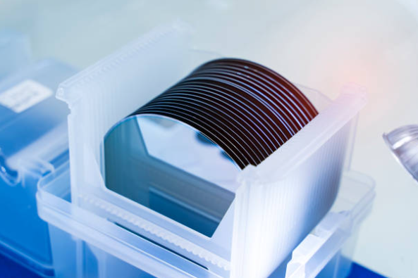
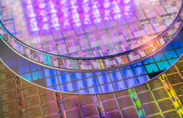
Figure 3-6. (a) An unprocessed semiconductor wafer (b) A wafer that has been processed to function as electronic circuits
The process of turning a wafer into chips is extremely complex, but here let’s touch on just the broad flow. When impurities are added to chosen parts of a semiconductor (a process technically called doping), the electrical properties of those parts change. Using this property and going through many processing steps, very small transistors can be built on the wafer. Then many layers of metal wiring, far thinner than a human hair, are stacked on top to connect the transistors to one another. By patterning the transistors and wiring together like this, a circuit of any desired form can be built on the wafer.
The transistor structure built on the wafer through doping and many other processes is the MOSFET (Metal-Oxide-Semiconductor Field-Effect Transistor), shown in Figure 3-7. As the last word of its name suggests, this structure acts, like the transistor we saw in Section 3.2, as a switch that opens and closes a path with voltage.
Let’s look a little more concretely. In the conceptual MOSFET structure in Figure 3-7 (a), the name Gate is used in place of B in Figure 3-4, and Drain and Source in place of C and E. When voltage is applied to the gate, the drain and source are connected and current flows; when it isn’t, they are disconnected. This is the same behavior as in the transistor component of Figure 3-4, where applying voltage to B connected C and E. The two devices differ in internal structure, but they are alike in being switches that open and close a path with voltage.
In other words, their function is the same; the difference is that the transistor in Figure 3-4 is large enough to see, while the MOSFET structures patterned on a wafer are so tiny they can’t be seen with the naked eye. Figure 3-7 (b) shows the structure of a MOSFET transistor as seen when looking inside a chip with an electron microscope — visible, quite literally, only through a high-powered microscope. That’s why transistors with this structure can be packed into a chip in enormous numbers. Packing countless transistors and their connecting wires densely onto a single small piece of semiconductor like this is technically called integration. (For reference, a circuit made this way is called an integrated circuit (IC), and what we call a chip is a kind of integrated circuit.)
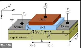
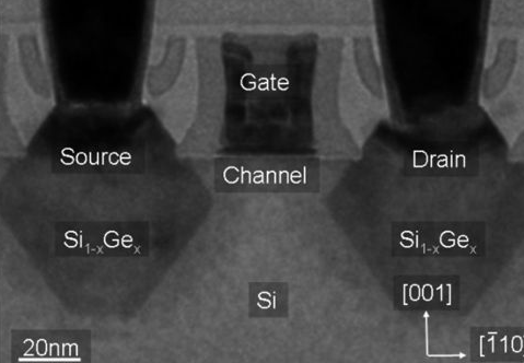
Figure 3-7. (a) Conceptual MOSFET structure (b) A transistor seen through an electron microscope
If you’ve followed this far, it should also make sense that a small chip with tens of billions of connected transistors can be made from a semiconductor wafer through many processing steps.
Generally, many copies of the same circuit are patterned on a single wafer. Each of the rectangles we saw in Figure 3-6 (b) is one such circuit. These rectangles are cut out one by one and then go through back-end steps such as packaging, which encases the semiconductor structure to protect it, to become the familiar-looking electronic components we call chips. That is why the inside of a CPU chip is made up of semiconductor-based MOSFET circuits. (Not every chip contains only transistors, however. Some chips, like DRAM, use a device called a capacitor alongside transistors; we’ll come back to this in Section 4.6.)
Although we’ve used the simple phrase “semiconductor processing,” going from a bare, unprocessed wafer to a chip that works as an electronic circuit involves an extremely complex and difficult series of steps. All of these steps together are called the semiconductor process, or fabrication. There are many important steps, but the core technological strength of semiconductor processing lies in how many transistors can be packed into how small an area. The more transistors you can pattern onto a chip of the same size, the larger and more complex the circuit it can hold. We’ll cover semiconductor processing in more detail later, in Chapter 9.
In this section, we’ve looked inside chips like the CPU. The chips we see are physically small, but inside them is a vast electronic circuit of tens of billions of connected transistors. From now on, when you look at a chip, I trust you’ll have gained the X-ray vision to see the finely etched circuits within.
Just as the steam engine and electricity sparked industrial revolutions that completely transformed the world, the technique of carving MOSFETs into semiconductors, and the arrival of the integrated circuit that gathers them onto a single chip, gave birth to the chip ecosystem and became the decisive events that made today’s computers and smart devices possible. This technology is also the fundamental reason the smartphones in our hands, and the data centers that run giant AI models, can exist at all.